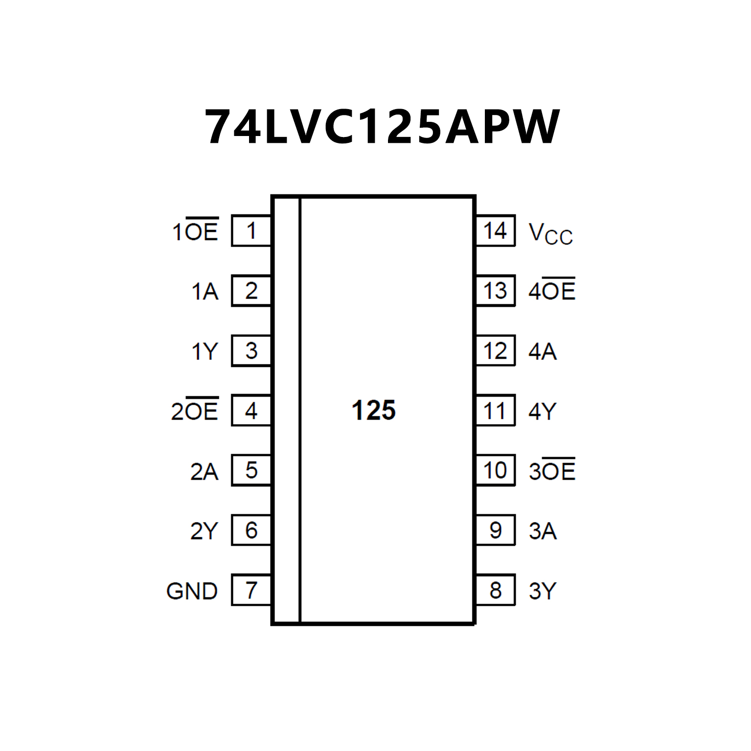






 74LVC125A.pdf
• Wide Supply Voltage Range: 1.65V to 3.6V
• Inputs Accept Voltages up to 5.5V
• Propagation Delay: 3.3ns (TYP) at VCC = 3.3V
• Output Ground Bounce VOLP (TYP) < 0.8V
at VCC = 3.3V and TA = +25℃
• Output VOH Undershoot VOHV (TYP) > 2V
at VCC = 3.3V and TA = +25℃
• 3-State Output
• Separate OE for All 4 Buffers
• Latch-up Performance Exceeds 250mA
• -40℃ to +125℃ Operating Temperature Range
• Available in Green SOIC-14 and TSSOP-14
Packages
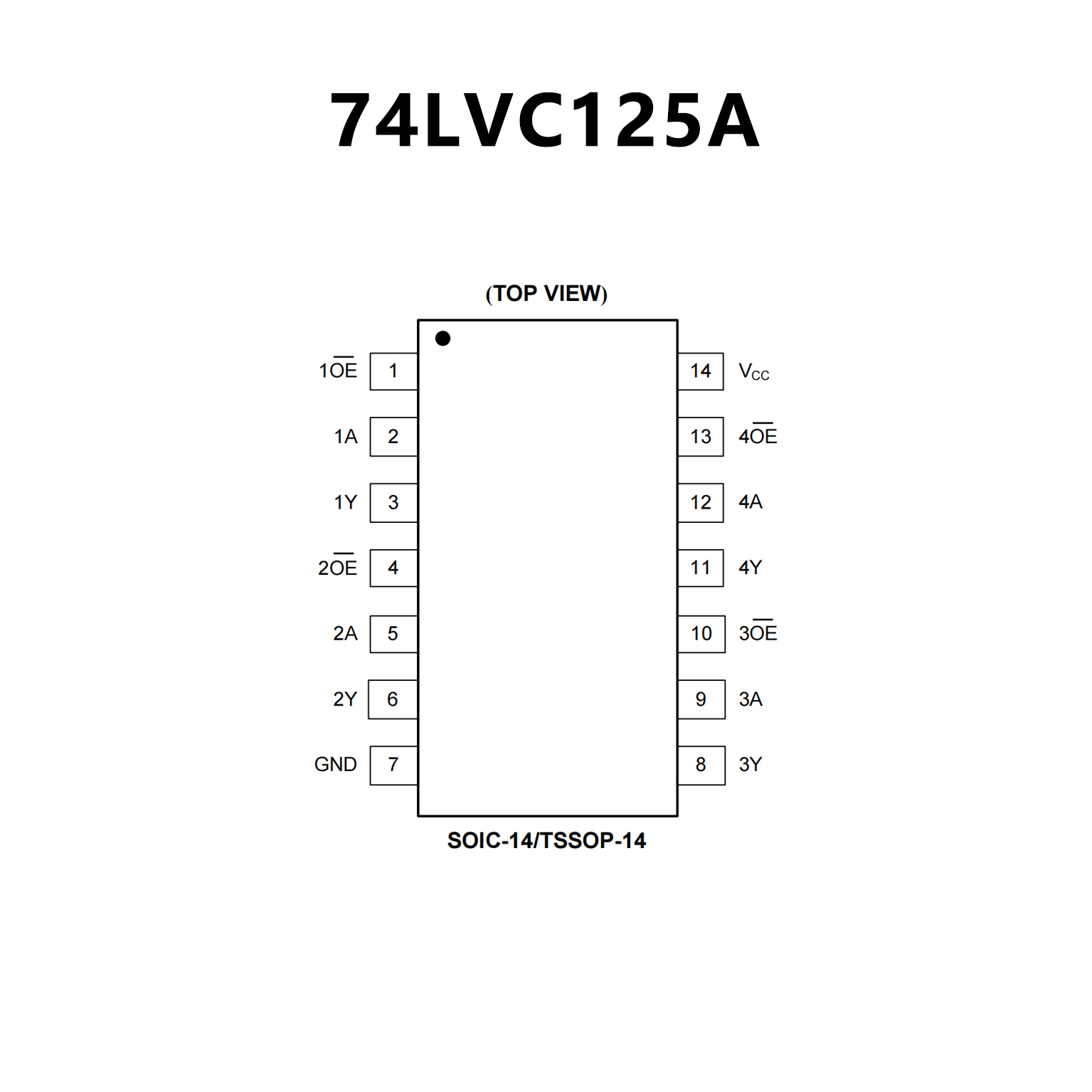
• Overvoltage tolerant inputs to 5.5 V
• Wide supply voltage range from 1.2 V to 3.6 V
• CMOS low power consumption
• Direct interface with TTL levels
• Complies with JEDEC standard:
• JESD8-7A (1.65 V to 1.95 V)
• JESD8-5A (2.3 V to 2.7 V)
• JESD8-C/JESD36 (2.7 V to 3.6 V)
• IOFF circuitry provides partial Power-down mode operation
• ESD protection:
• HBM JESD22-A114F exceeds 2000 V
• MM JESD22-A115-B exceeds 200 V
• CDM JESD22-C101E exceeds 1000 V
• Multiple package options
• Specified from -40 °C to +85 °C and -40 °C to +125 °C