


Sink/Source DDR Termination Regulator, EUP7998 Replace SQ24335.
EUP7998 EUP7998.pdf
EUP7998.pdfFEATURES
• VLDOIN Input Voltage Range: 1.1V to 3.5V
• VIN Input Voltage Range: 2.375V to 5.5V
• Typically 3×10μF MLCCs stable for DDR
• Fast Load-Transient Response
• ±10mA Buffered Reference (REFOUT)
• Meet DDR, DDR2 JEDEC Specifications.
Supports DDR3 and Low-Power DDR3/DDR4
VTT Applications
• Power-Good Window Comparator
• With Soft Start, UVLO and OCP
• Thermal Shutdown
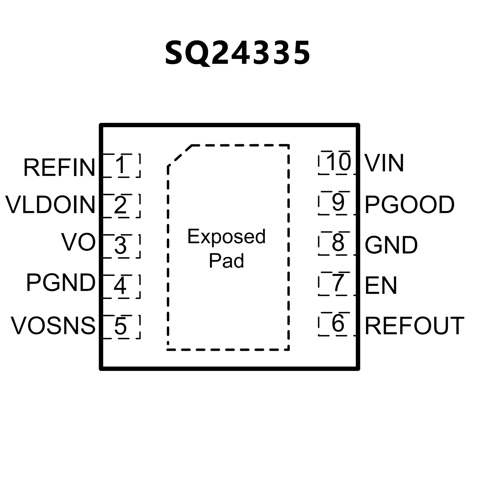
• Available in 10-Pin 3mm×3mm TDFN and
SOP-8 (EP) packages
• RoHS Compliant and 100% Lead(Pb)-Free
Halogen-Free
PIN CONFIGUTION
优势替代
FEATURES
• Input Voltage: Supports 2.5V Rail and 3.3V Rail
• VLDOIN Voltage Range: 1.1V to 3.5V
• Sink and Source Termination Regulator
Includes Droop Compensation.
• Requires Minimum Output Capacitance of 20µF
(Typically 3×10µF MLCCs) for Memory.
• PGOOD to Monitor Output Regulation
• Enable Function Option
• REFIN Input Allows for Flexible Input Tracking
either Directly or Through Resistor Divider
• Remote Sensing(VOSNS)
• ±10mA Buffered Reference(REFOUT)
• Built-in Soft-start, UVLO, and OCL
• Thermal Shutdown Protection
• Supports DDR, DDR2, DDR3, DDR3L, Low
Power DDR3, DDR4 VTT Applications
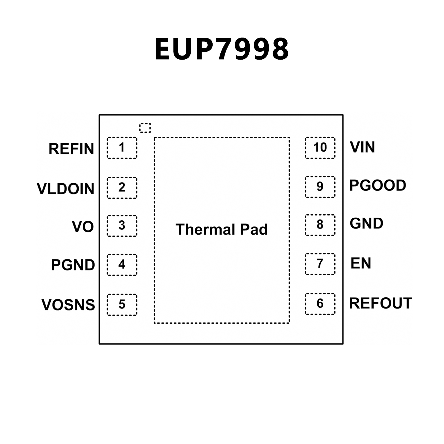
• Compacted Package: DFN3×3-10 with Thermal
Pad
PIN CONFIGUTION