


 SGM48521Q.pdf
• AEC-Q100 Qualified for Automotive Applications
Device Temperature Grade 1
TA = -40℃ to +125℃
• 5V Supply Voltage
• 7A Peak Source and 6A Peak Sink Currents
• Ultra-Fast, Low-side Gate Driver for GaN and Si
FETs
• Minimum Input Pulse Width: 1ns
• Up to 60MHz Operation
• Propagation Delay: 2.2ns (TYP), 3.5ns (MAX)
• Rise Time:
WLCSP-0.88×1.28-6B: 500ps (TYP)
TDFN-2×2-6DL: 600ps (TYP)
• Fall Time:
WLCSP-0.88×1.28-6B: 460ps (TYP)
TDFN-2×2-6DL: 590ps (TYP)
• Protection Features:
Under-Voltage Lockout (UVLO)
Over-Temperature Protection (OTP)
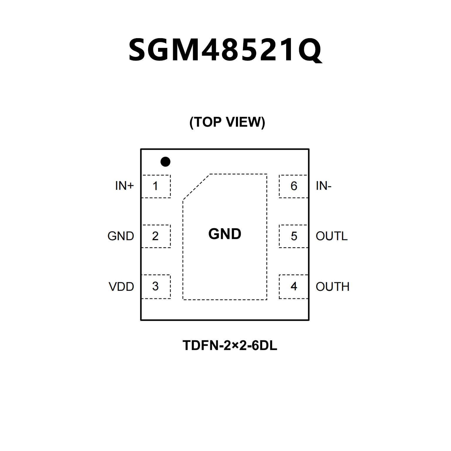
• Available in Green WLCSP-0.88×1.28-6B and
TDFN-2×2-6DL Packages
• AEC-Q100 grade 1 qualified
• 1.25-ns typical minimum input pulse width
• 2.6-ns typical rising propagation delay
• 2.9-ns typical falling propagation delay
• 300-ps typical pulse distortion
• Independent 7-A pull-up and 5-A pull-down current
• 650-ps typical rise time (220-pF load)
• 850-ps typical fall time (220-pF load)
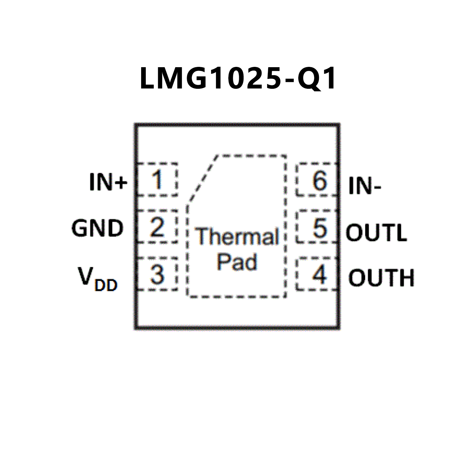
• 2-mm x 2-mm QFN package
• Inverting and non-inverting inputs
• UVLO and over-temperature protection
• Single 5-V supply voltage