


 SGM48526.pdf
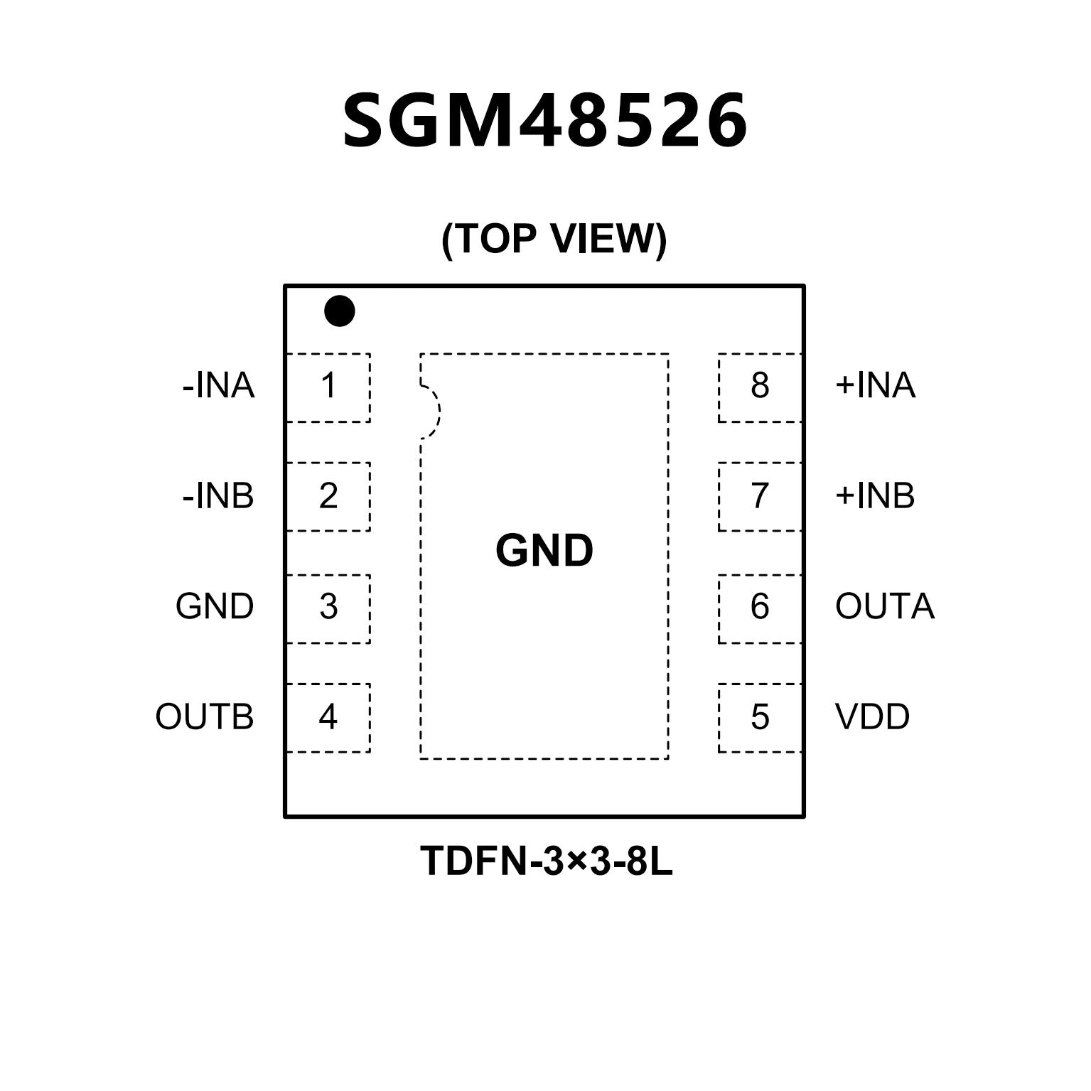
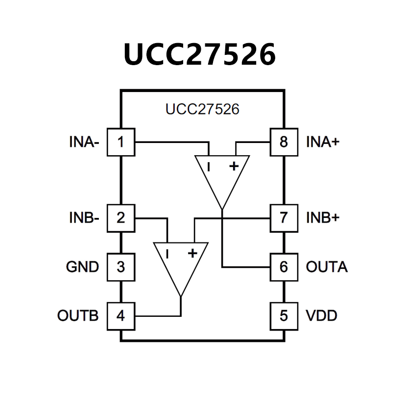
• Industry-Standard Pinout
• Two Independent Gate-Drive Channels
• 5-A Peak Source and Sink-Drive Current
• Independent-Enable Function for Each Output
TTL and CMOS Compatible Logic Threshold
Independent of Supply Voltage
• Hysteretic-Logic Thresholds for High Noise Immunity
• Inputs and Enable Pin-Voltage Levels
Not Restricted by VDD Pin Bias Supply Voltage
• 4.5-V to 18-V Single-Supply Range
• Outputs Held Low During VDD-UVLO,
(Ensures Glitch-Free Operation at
Power up and Power Down)
• Fast Propagation Delays (13-ns Typical)
• Fast Rise and Fall Times (7-ns and 6-ns Typical)
• 1-ns Typical Delay Matching Between Two Channels
• Two Outputs are in Parallel for Higher Drive Current
• Outputs Held Low When Inputs Floating
• PDIP (8), SOIC (8), MSOP (8) PowerPAD™ and
3-mm × 3-mm WSON-8 Package Options
• Operating Temperature Range of –40°C to 140°C