


P-Channel Enhancement Mode Field Effect Transistor
PM569BA
 PM569BA.pdf
PM569BA.pdf
No.11074
FEATURES
• V(BR)DSS: -40V
• RDS(ON): 70mΩ
• ID: -2.5A
DESCRIPTION
• Pb−Free, Halogen Free and RoHS compliant.
• Low RDS(on) to Minimize Conduction Losses.
• Ohmic Region Good RDS(on) Ratio.
• Optimized Gate Charge to Minimize Switching Losses.
APPLICATION CIRCUIT
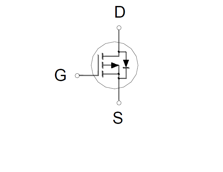
PIN CONFIGUTION