


 SGM4566.pdf
No.11050
● 1.2V to 5.5V on A Ports and 1.65V to 5.5V on B Ports (VCCA ≤ VCCB)
● VCC Isolation: If Either VCC is at GND, All Outputs are in the
High-Impedance State
● OE Input Circuit Referenced to VCCA
● Low Power Consumption
● Push-Pull Output
● IOFF: Supports Partial-Power-Down Mode Operation
● -40℃ to +85℃ Operating Temperature Range
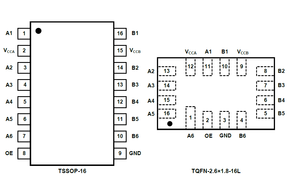
● Available in Green TSSOP-16 and TQFN-2.6×1.8-16L Packages
This 6-bit non-inverting voltage-level translator uses two separate configurable power-supply rails. The A ports are designed to track VCCA. VCCA accepts any supply voltage from 1.2V to 5.5V. The B ports are designed to track VCCB. VCCB accepts any supply voltage from 1.65V to 5.5V. This allows for universal low-voltage bidirectional translation between any of the 1.2V, 1.5V, 1.8V, 2.5V, 3.3V, and 5V voltage nodes. VCCA should not exceed VCCB. When the output-enable (OE) input is low, all outputs are placed in the high-impedance state. To ensure the high-impedance state during power up or power down, OE should be tied to GND through a pull-down resistor; the minimum value of the resistor is determined by the current-sourcing capability of the driver.
The SGM4566 is designed so that the OE input circuit is supplied by VCCA. This device is fully specified for partial-power-down applications using IOFF. The IOFF circuitry disables the outputs, preventing damaging current backflow through the device when it is powered down.