





 SGM4552.pdf
No.11058
● No Direction-Control Signal Needed
● Data Rates
24Mbps (Push-Pull)
2Mbps (Open-Drain)
● 1.65V to 5.5V on A Port and 2.3V to 5.5V on B Port
(VCCA ≤ VCCB)
● VCC Isolation: If Either VCC is at GND, Both Ports are
in the High-Impedance State
● No Power-Supply Sequencing Required: Either VCCA or
VCCB can be Ramped First
● IOFF: Supports Partial-Power-Down Mode Operation
● Available in Green UTDFN-1.45×1-6L, SOT-23-6 and SC70-6 Packages
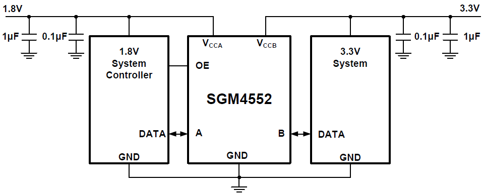
This one-bit non-inverting translator uses two separate configurable power-supply rails. The A port is designed to track VCCA. VCCA accepts any supply voltage from 1.65V
to 5.5V. The B port is designed to track VCCB. VCCA must be less than or equal to VCCB. VCCB accepts any supply voltage from 2.3V to 5.5V. This allows for low voltage bidirectional translation between any of the 1.8V, 2.5V, 3.3V, and 5V voltage nodes. When the output-enable (OE) input is low, all outputs are placed in the high-impedance state, which significantly reduces the power-supply quiescent current consumption. OE has an internal pull-down current source, as long as VCCA is powered.
To ensure the high-impedance state during power up or power down, OE should be tied to GND through a pull-down resistor; the minimum value of the resistor is determined by the current-sourcing capability of the driver.