 SGM48521Q.pdf
No.14087
• AEC-Q100 Qualified for Automotive Applications
Device Temperature Grade 1
TA = -40℃ to +125℃
• 5V Supply Voltage
• 7A Peak Source and 6A Peak Sink Currents
• Ultra-Fast, Low-side Gate Driver for GaN and Si FETs
• Minimum Input Pulse Width: 1ns
• Up to 60MHz Operation
• Propagation Delay: 2.2ns (TYP), 3.5ns (MAX)
• Rise Time:
WLCSP-0.88×1.28-6B: 500ps (TYP)
TDFN-2×2-6DL: 600ps (TYP)
• Fall Time:
WLCSP-0.88×1.28-6B: 460ps (TYP)
TDFN-2×2-6DL: 590ps (TYP)
• Protection Features:
Under-Voltage Lockout (UVLO)
Over-Temperature Protection (OTP)
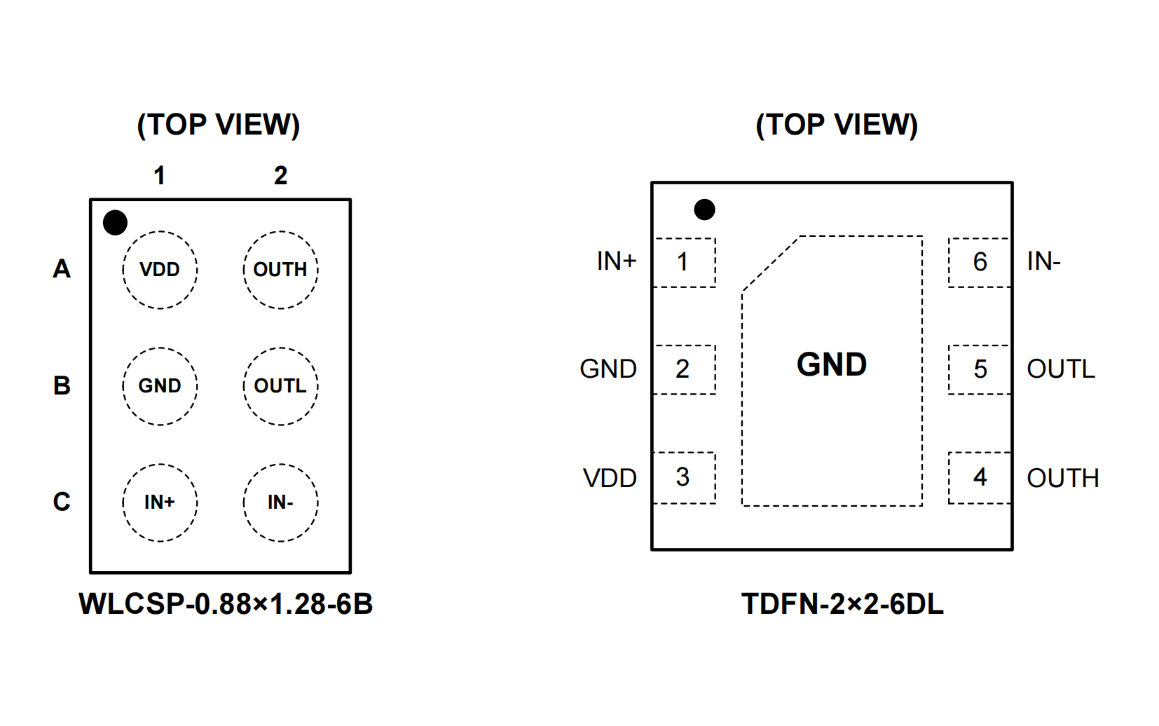
• Available in Green WLCSP-0.88×1.28-6B and
TDFN-2×2-6DL Packages
The high-speed, single-channel low-side driver SGM48521Q is designed to drive GaN FETs and logic level MOSFETs. Application areas include LiDAR, time of flight, facial recognition, and power converters using low-side drivers. The SGM48521Q provides 7A source and 6A sink output current capability. Split output configuration allows individual turn-on and turn-off time optimization depending on FET. Package and pinout with minimum parasitic inductances reduce the rise and fall time and limit the ringing. Additionally, the 2.2ns propagation delay with minimized tolerances and variations allows efficient operation at high frequencies.


