


 N5100V.pdf
No.11070
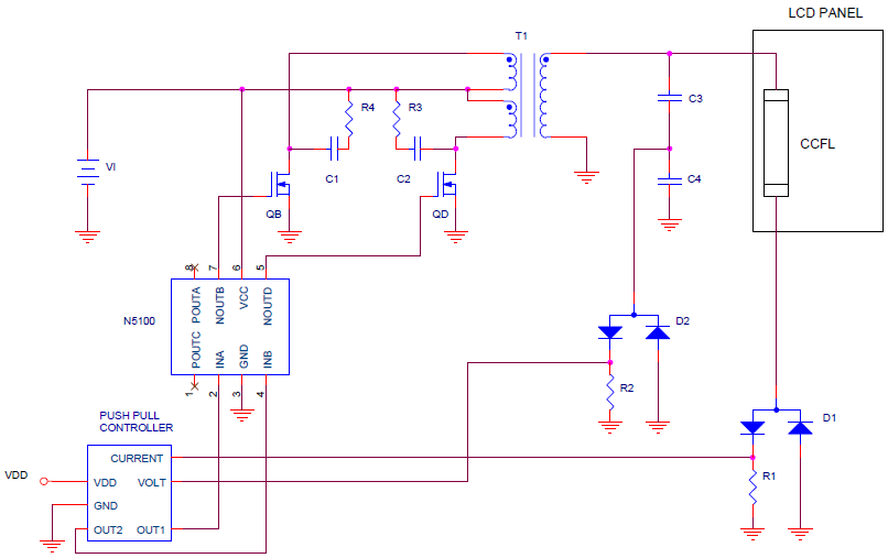
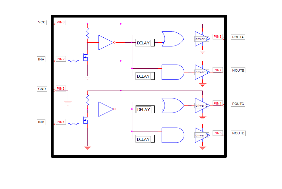
• POUTC ( Pin 1 ) : The output of driver C that is driving the external
P-channel MOSFET.
• INA ( Pin 2 ) : The control input A; TTL/CMOS compatible input.
• GND( Pin 3 ) : The GND pin.
• INB( Pin 4 ) : The control input B; TTL/CMOS compatible input.
• NOUTD ( Pin 5) : The output of driver D that is driving the external
N-channel MOSFET.
• VCC (Pin 6) : Supply voltage input.
• NOUTB ( Pin 7 ) : The output of driver B that is driving the external
N-channel MOSFET.
• POUTA ( Pin 8 ) : The output of driver A that is driving the external
P-channel MOSFET.
The N5100 is a universal switching buffer with strong functions, specifically designed to drive the power MOSFET for the various switching topology applications, it allows to receive dual input signals from a push-pull controller, and transfer to provide total 4 driving outputs for directly driving dual N-channel and dual P-channel MOSFETs.
The N5100 is suitable for DC/DC converter or DC/AC inverter applications. It is operating in high efficiency ZVS control while used in the DC/AC application.
The N5100 provides 4 high current totem pole outputs that allow to be used on the multiple switching control application with single universal switching buffer.