


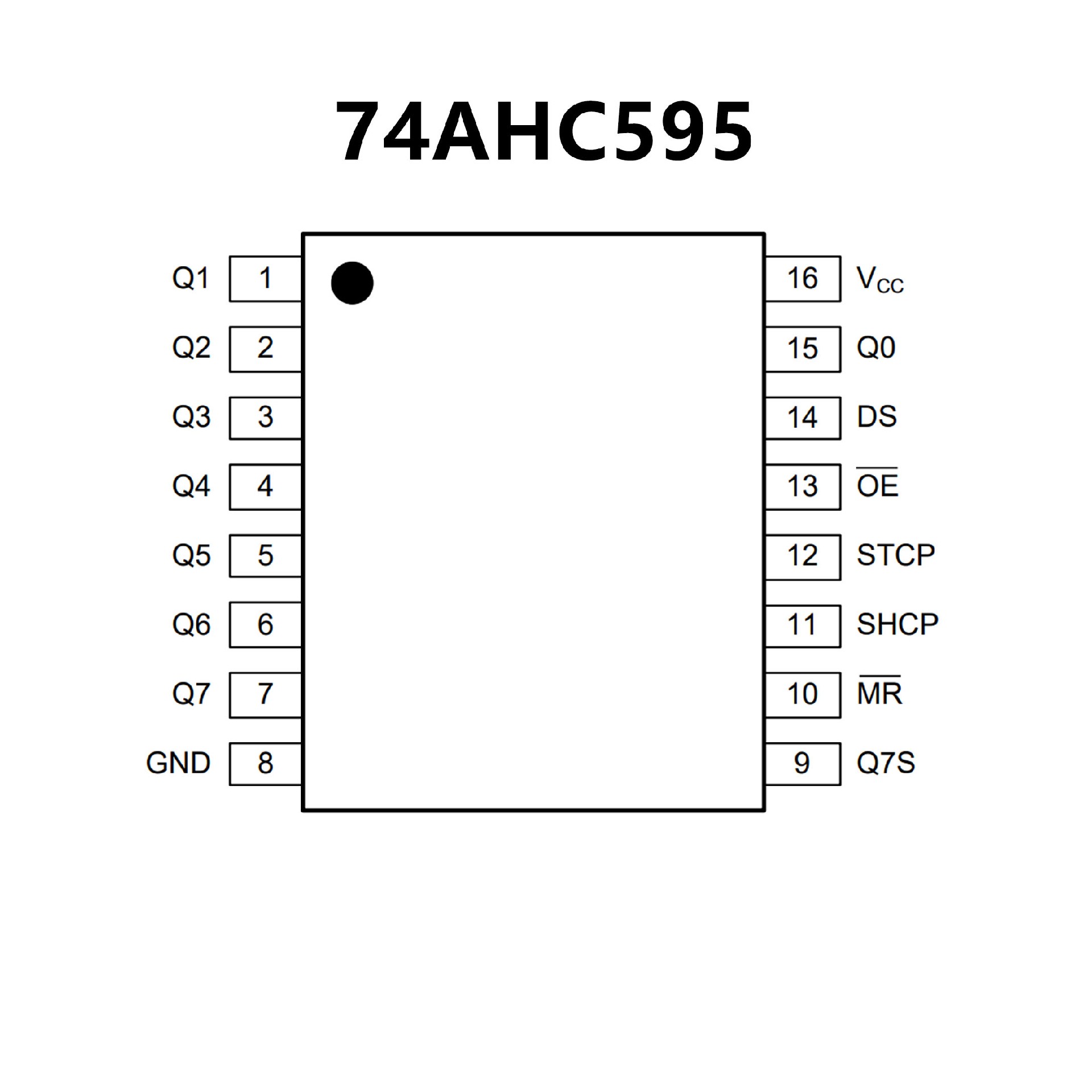
 74AHC595.pdf
• Balanced Propagation Delays
• All Inputs Have Schmitt-Trigger Action
• Inputs Accept Voltages Higher than VCC
• Operates with CMOS Input Levels
• -40℃ to +125℃ Operating Temperature Range
• Available in a Green TSSOP-16 Package
• Output Drive Capability: 15 LSTTL Loads
• Outputs Directly Interface to CMOS, NMOS, and TTL
• Operating Voltage Range: 2.0 to 6.0 V
• Low Input Current: 1.0 µA
• High Noise Immunity Characteristic of CMOS Devices
• In Compliance with the Requirements
Defined by JEDEC Standard No. 7 A
• Chip Complexity: 328 FETs or 82 Equivalent Gates
• Improvements over HC595
Improved Propagation Delays
50% Lower Quiescent Power
Improved Input Noise and Latchup Immunity
• NLV Prefix for Automotive and Other Applications Requiring
Unique Site and Control Change Requirements;
AEC−Q100 Qualified and PPAP Capable
• These Devices are Pb−Free, Halogen
Free and are RoHS Compliant