 74LVC1T45.pdf
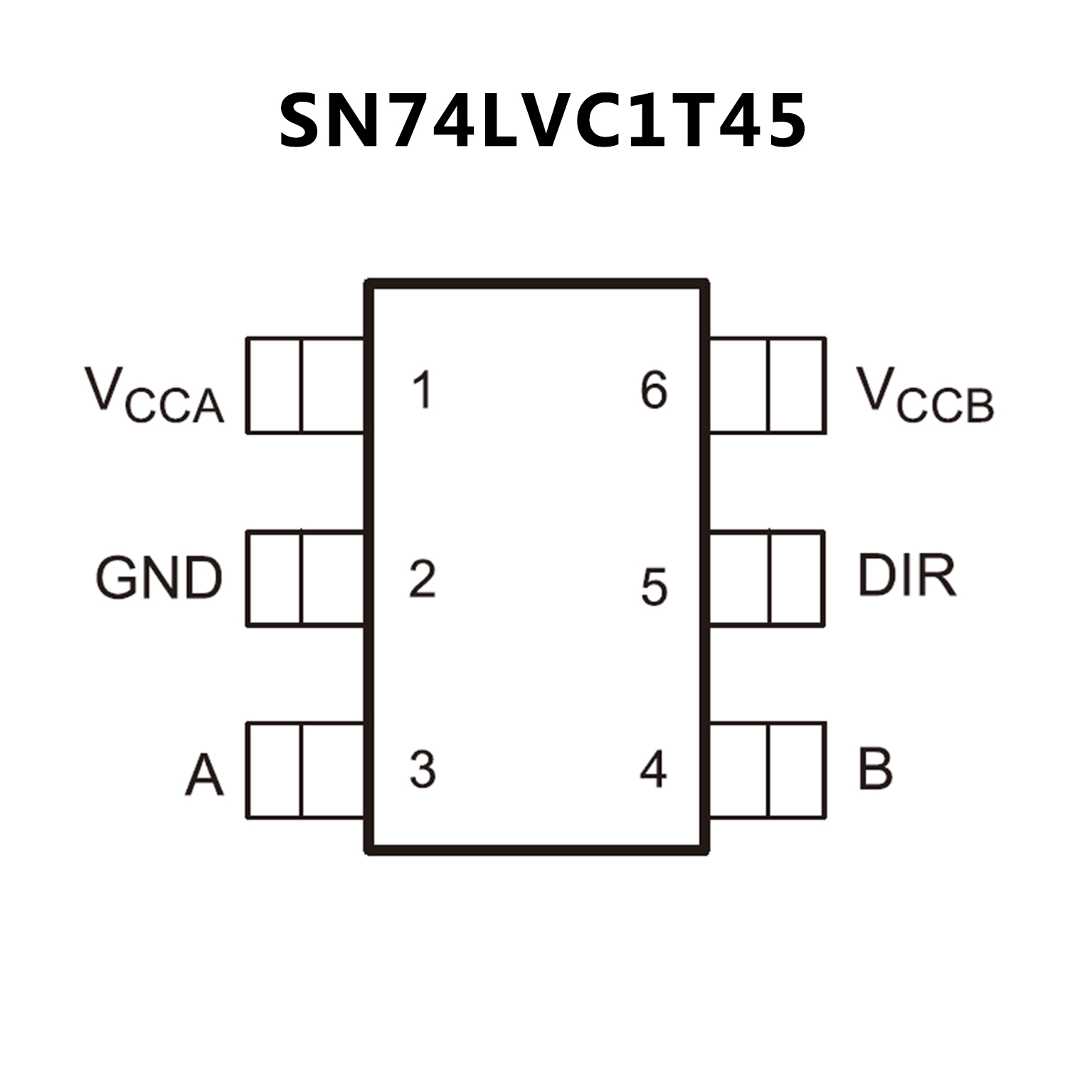
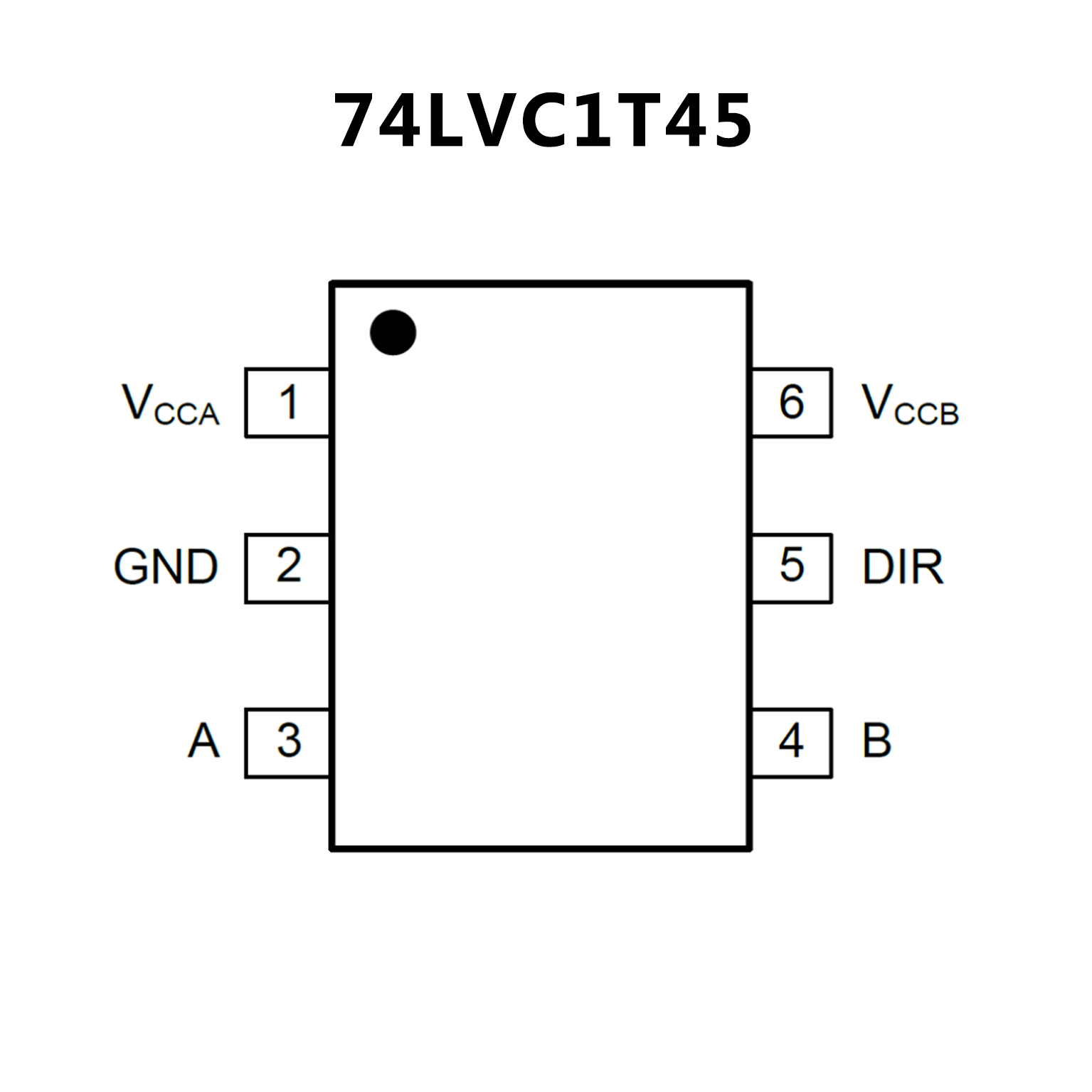
• VCCA Supply Voltage Range: 1.65V to 5.5V
• VCCB Supply Voltage Range: 1.65V to 5.5V
• DIR Input Circuit Referenced to VCCA
• +32mA/-32mA Output Current
• Data Rates
420Mbps (3.3V to 5V Translation)
210Mbps (Translate to 3.3V)
140Mbps (Translate to 2.5V)75Mbps (Translate to 1.8V)
• Outputs in High-Impedance State when VCCA or VCCB = 0V
• -40℃ to +125℃ Operating Temperature Range
• Available in Green SC70-6, SOT-23-6 Packages
• ESD Protection Exceeds JESD 22
2000-V Human-Body Model (A114-A)
200-V Machine Model (A115-A)
1000-V Charged-Device Model (C101)
• Available in the Texas Instruments NanoFree™ Package
• Fully Configurable Dual-Rail Design Allows Each Port to
Operate Over the Full 1.65-V to 5.5-V Power-Supply Range
• VCC Isolation Feature – If Either VCC Input Is at GND,
Both Ports Are in the High-Impedance State
• DIR Input Circuit Referenced to VCCA
• Low Power Consumption, 4-µA Max ICC
• ±24-mA Output Drive at 3.3 V
• Ioff Supports Partial-Power-Down Mode Operation
• Max Data Rates
420 Mbps (3.3-V to 5-V Translation)
210 Mbps (Translate to 3.3 V)
140 Mbps (Translate to 2.5 V)
75 Mbps (Translate to 1.8 V)
• Latch-Up Performance Exceeds
100 mA Per JESD 78, Class II
