


 74LVC2G04.pdf
• Wide Operating Voltage Range: 2.7V to 3.6V
• Input and Output Interface Capability to 5V
System Environment
• +64mA/-32mA Output Current
• 3-State Outputs Drive Bus Lines Directly
• Power-up and IOFF 3-State
• Bus Hold-on Data Inputs with No Need for
External Pull-up/Pull-down Resistors
• -40℃ to +125℃ Operating Temperature Range
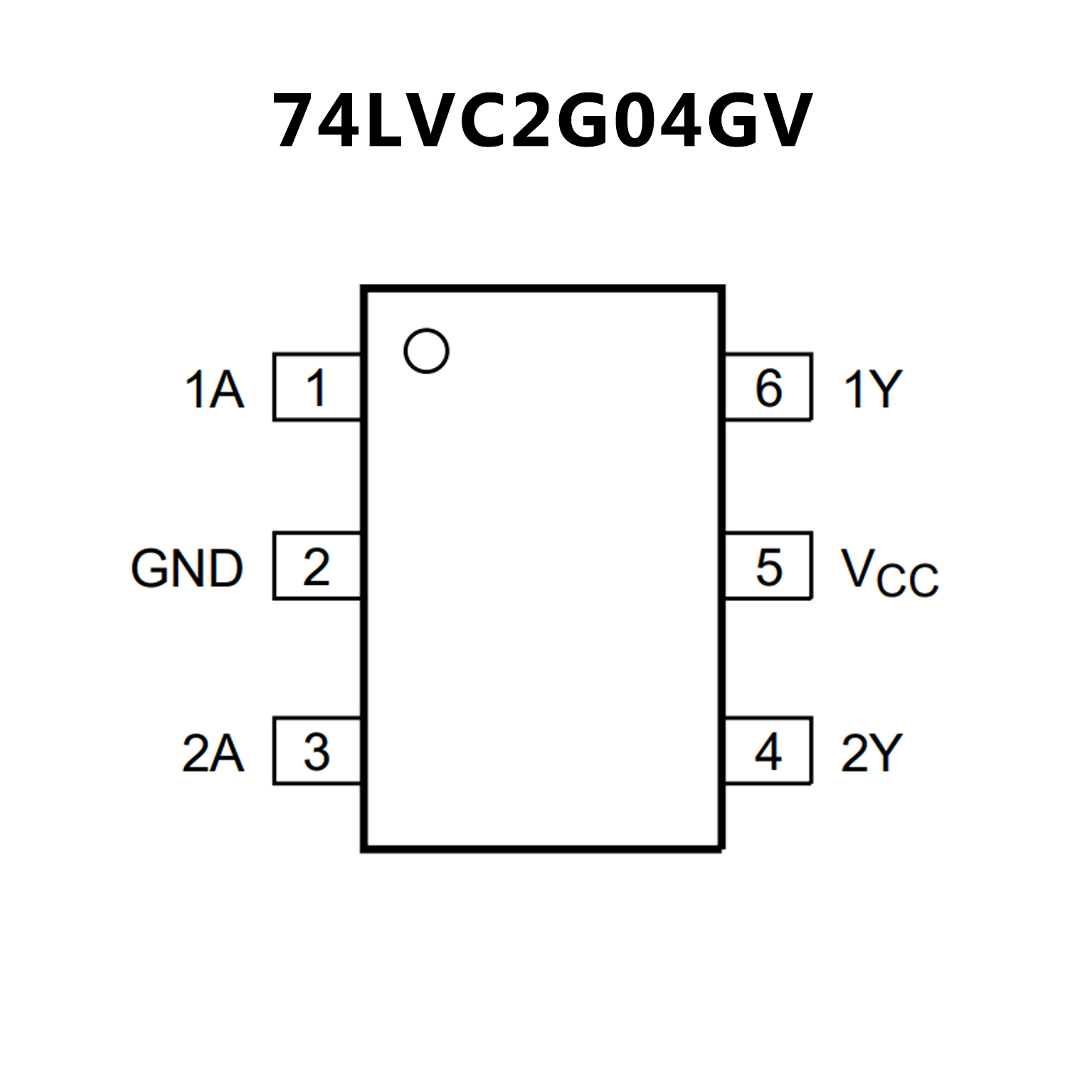
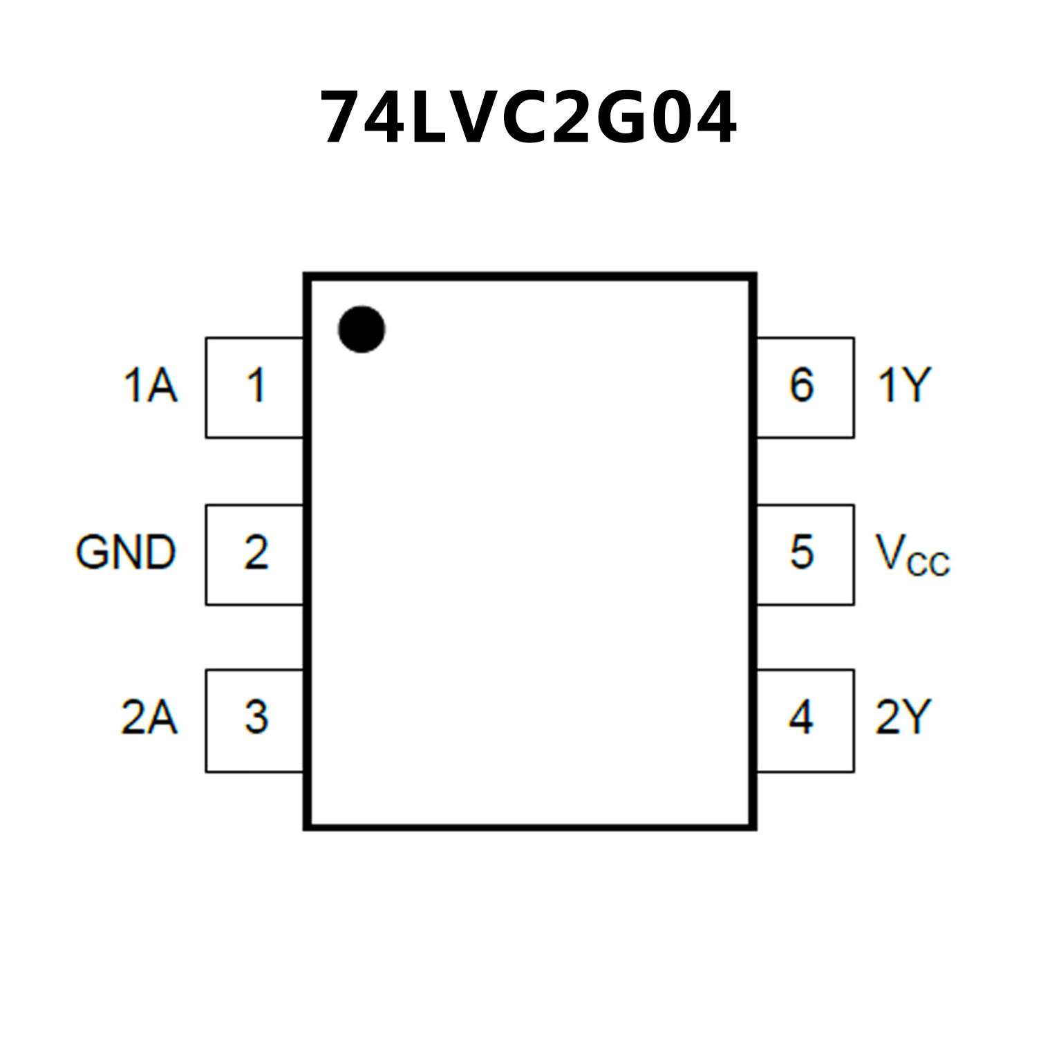
• Available in a Green TQFN-4.5×2.5-20L Package
• Automotive product qualification in accordance with AEC-Q100 (Grade 1)
• Specified from -40 °C to +85 °C and from -40 °C to +125 °C
• 5 V tolerant inputs/outputs for interfacing with 5 V logic
• Wide supply voltage range from 1.2 V to 3.6 V
• CMOS low-power consumption
• Direct interface with TTL levels
• Overvoltage tolerant inputs to 5.5 V
• Bus hold on all data inputs (74LVCH245A-Q100 only)
• IOFF circuitry provides partial Power-down mode operation
• Complies with JEDEC standard: • JESD8-7A (1.65 V to 1.95 V)
• JESD8-5A (2.3 V to 2.7 V)
• JESD8-C/JESD36 (2.7 V to 3.6 V)
• ESD protection:
MIL-STD-883, method 3015 exceeds 2000 V
HBM JESD22-A114F exceeds 2000 V
MM JESD22-A115-A exceeds 200 V (C = 200 pF, R = 0 Ω)
• DHVQFN package with Side-Wettable Flanks enabling Automatic
Optical Inspection (AOI) of solder joints