Low Noise Operational Amplifier,SGM8632 Replace TLC272.
SGM8632 SGM8632.pdf
 SGM8632.pdf
FEATURES
• Rail-to-Rail Input and Output
• 3.5mV Maximum Input Offset Voltage
• High Gain-Bandwidth Product: 6MHz
• High Slew Rate: 3.7V/μs
• Settling Time to 0.1% with 2V Step: 0.5μs
• Overload Recovery Time: 0.9μs
• Low Noise: 13nV/ Hz at 1kHz
• Supply Voltage Range: 2V to 5.5V
• Input Voltage Range: -0.1V to +5.6V with VS = 5.5V
• Low Supply Current: 480μA/Amplifier (TYP)
• Available in Green MSOP-8 Package
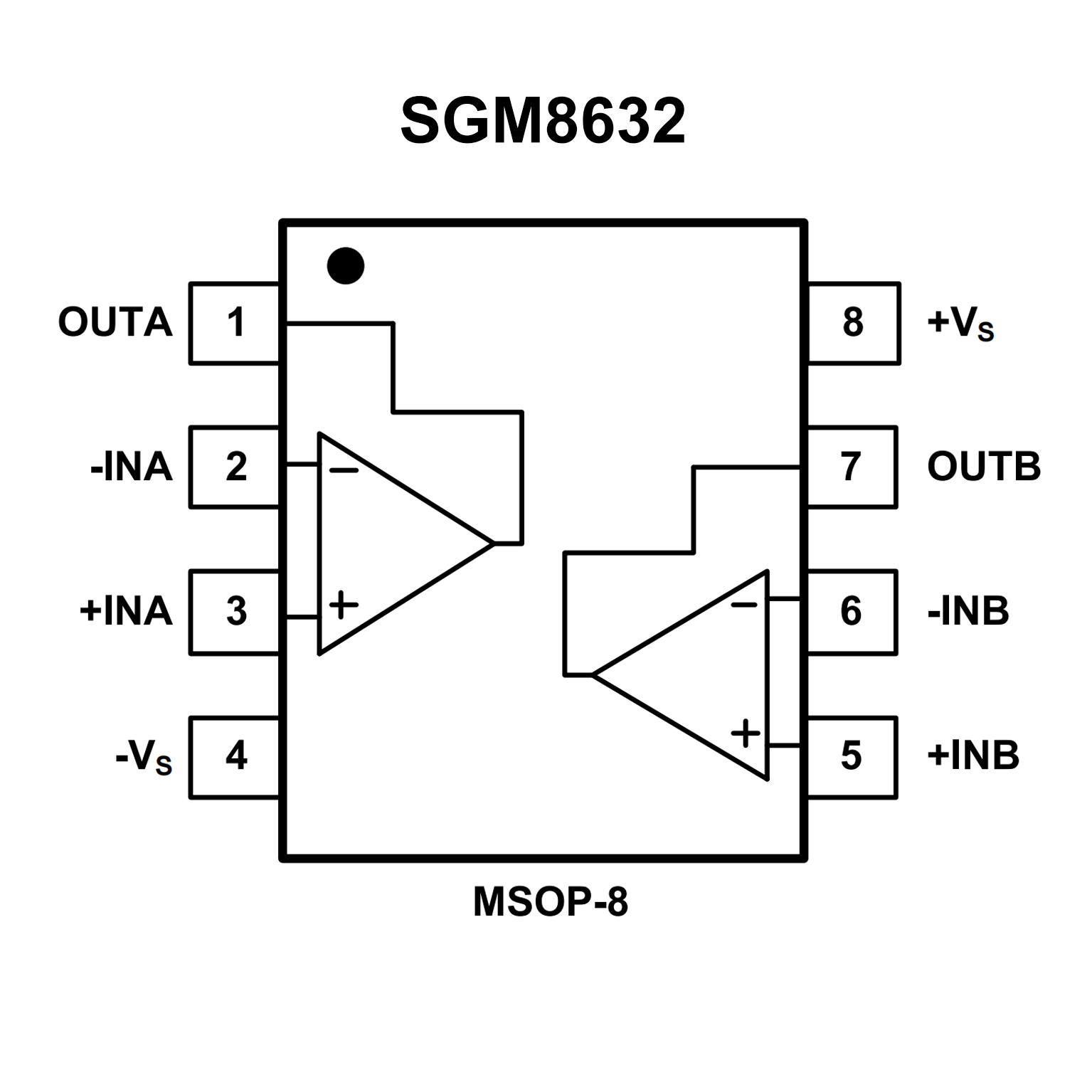
PIN CONFIGUTION

优势替代
FEATURES
• Trimmed Offset Voltage:TLC277 . . . 500 µV Max at 25°C,
VDD = 5 V
• Input Offset Voltage Drift ...Typically
0.1 µV/Month, Including the First 30 Days
• Wide Range of Supply Voltages Over
Specified Temperature Range:
0°C to 70°C . . . 3 V to 16 V
–40°C to 85°C . . . 4 V to 16 V
–55°C to 125°C . . . 4 V to 16 V
• Single-Supply Operation
• Common-Mode Input Voltage Range Extends Below the
Negative Rail (C-Suffix,I-Suffix types)
• Low Noise ...Typically 25 nV/√Hz at f = 1 kHz
• Output Voltage Range Includes Negative Rail
• High Input impedance . . . 1012 Ω Typ
• ESD-Protection Circuitry
• Small-Outline Package Option Also Available in Tape and Reel
• Designed-In Latch-Up Immunity
PIN CONFIGUTION


